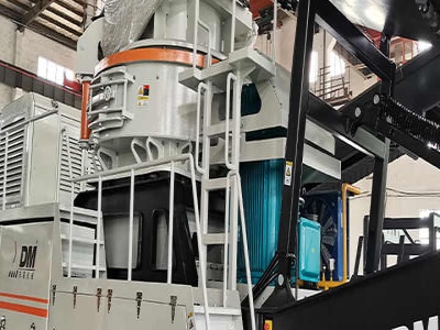
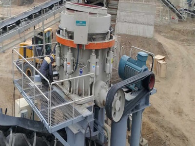
CVD Processes and Equipment Introduction Closed and Open Reactor Reactant Supply Thermal CVD: Deposition System and Reactor Design Exhaust and ByProduct Disposal Laser and Photo CVD Chemical Vapor Infiltration (CVI) FluidizedBed CVD Plasma CVD References.
Growth rate predictions of chemical vapor deposited silicon carbide epitaxial layers. Ö. Danielsson, A. Henry and E. Janzén Journal of Crystal Growth, vol. 243 (2002) 170 – 184. Predicted nitrogen doping concentrations in silicon carbide epitaxial layers grown by hotwall chemical vapor deposition. Ö. Danielsson, U. Forsberg and én
Layered Hafnium Carbide/Silicon Carbide. Hard, wearresistant, chemically inert, chemically resistant, and nearly impervious to hydrogen at high temperatures, refractory carbides can be formed by chemical vapor deposition at temperatures as low as 10% of their melting point. Ultramet offers the following materials, along with other carbides, nitrides, and silicides:
To realize the supersmooth polishing of chemical vapor deposition silicon carbide(CVD SiC),nanoscratch test is applied to study the critical load for brittleductile transition,and its polishing mechanism is analyzed according to the force on an abrasive grain.
of silicon carbide, as well as other ceramics, quartz, and metals in chemical seals and bearings, equipment components, semiconductor waferhandling and chamber components, optical components and other demanding applications. Advanced Materials' bulk chemical vapor deposition (CVD) process produces freestanding monolithic CVD SILICON CARBIDE.
Layered Hafnium Carbide/Silicon Carbide. Hard, wearresistant, chemically inert, chemically resistant, and nearly impervious to hydrogen at high temperatures, refractory carbides can be formed by chemical vapor deposition at temperatures as low as 10% of their melting point.
Its chemical formula is SiC. Since the late 19th century silicon carbide has been an important material for sandpapers, grinding wheels, and cutting tools. More recently, it has found application in refractory linings and heating elements for industrial furnaces, in wearresistant parts for pumps and rocket engines,...
puter chips, light emitting diodes (LEDs), communication technology, and radar. systems, are achieved by growing thin films of materials above a common substrate. An established method of choice for thin film growth is chemical vapor deposition. (CVD).
Silicon carbide is extremely hard, with low density, low thermal expansion and high thermal shock resistance. Not susceptible to harm by molten salts, alkalis or acids, it also displays extremely high levels of chemical inertness. Because of its superior characteristics, silicon carbide can be labeled as an engineering, technical or advanced ceramic.
Amorphous silicon carbide (a‐SiC) films, deposited by plasma‐enhanced chemical vapor deposition (PECVD), have been evaluated as insulating coatings for implantable microelectrodes. The a‐SiC was deposited on platinum or iridium wire for measurement of electrical leakage through the coating in phosphate‐buffered saline (PBS, pH ).
7. Mitchenko, Tarala. Equipment for growing silicon carbide films by chemicalgas vapor deposition // Materials of XXXIV scientific conference on the results of the work of professors and graduate students. 2005, p. 9294. 8. S. Madapura, Steckl, and M. Loboda.
Epitaxial growth of rhombohedral boron nitride (rBN) on different polytypes of silicon carbide (SiC) is demonstrated using thermally activated hotwall chemical vapour deposition and triethyl boron and ammonia as precursors. With respect to the crystalline quality .
SUPERSiC silicon carbide contains about 18% residual porosity, providing a substrate core that is inherently lightweight. Applying an encapsulating or selectively placed coating completes the substrate's preparation. POCO offers three coatings as a polishing surface: Chemical Vapor Deposition...
Silicon carbide (SiC; βtype) plates were prepared by a chemical vapor deposition technique using SiCl 4, C 3 H 8 and H 2 as source gases under the following conditions: deposition temperature (T dep); 1300°1800°C, total gas pressure (P tot); 30760Torr and C 3 H 8 gas flow rate [FR(C 3 H 8)]; 1090cm 3 /min, and the effects of FR(C 3 H 8) on the carbon content, density, crystal structure ...
Chemical vapor deposition at atmospheric pressure is as old as CVD itself and, indeed, up until the late 1970s virtually all epitaxial silicon deposition was done using VD . VD is characterized by film deposition in the transportlimited regime, high gas flows, and, because vacuum equipment is not required, low equipment cost.
Principal/ Sr. Principal Physical Vapor Deposition (PVD )Process Engineer in Moses Lake, WA ... Gallium Nitride, Silicon Carbide, Carbon Nanotubes) and providing leading edge technology ...
Pitsiri Sukkaew, Emil Kalered, Erik Janzén, Olof Kordina, Örjan Danielsson, and Lars Ojamäe . Growth Mechanism of SiC Chemical Vapor Deposition: Adsorption and Surface Reactions of Active Si Species. The Journal of Physical Chemistry C 2018, 122 (1), 648661.
Hot filament CVD also has a number of advantages over proven plasmaassisted coating methods for the production of siliconbased films: The technology and its benefits. Chemical precipitation of films from the gas phase (chemical vapour deposition, CVD) following activation of the reactive gas on hot filaments; High gas yields; High coating rates
Luminescence and Structure of ZnO Grown by Physical Vapor Deposition: Quantum Hall resistance standards from graphene grown by chemical vapor deposition on silicon carbide: PROPERITES OF HYDROGENATED AMORPHOUS SILICON CARBIDE FILMS IRRADIATED BY EXCIMER PULSE LASER: PlasmaAssisted Chemical Vapor Deposition of Titanium Oxide Layer at RoomTemperature
Performance SiC, conductive CVD silicon carbide gives equipment manufacturers new options for materials to use in the processing chamber. The benefits of CVD silicon carbidepurity, stiffness, chemical and oxidation resistance, ability to withstand thermal shock, and dimensional stability—now combine with low electrical resistance, opening up the door to new ways to process wafers.
Size distribution and single particle characterization of airborne particulate matter collected in a silicon carbide plant. Recovery of cutting fluids and silicon carbide from slurry waste. Structural, chemical, and magnetic properties of cobalt intercalated graphene on silicon carbide.
PECVD Amorphous Silicon Carbide (αSiC) Layers for ... chemical vapor deposition (PECVD) of SiC in an amorphouos state (αSiC) can be such a ... In most of the cases, the equipment is used for multiple depositions such as SiO2 (doped and undoped), Si3N4, αSi or even TEOS (using a special
Silicon carbide (SiC) coating is deposited on C/C composite substrate for the first time by chemical vapor deposition (CVD) with hexamethyldisilylamine (HMDS, C 6 H 19 NSi 2) as precursor and N 2 as carrier gas in an intermediate deposition temperature range. The effects of deposition temperature on phase constitution, surface morphology and deposition rate of the coating are investigated by ...
Equipment name Badger ID Purpose(s) Cleaning Required ... Plasma Enhanced (PE) CVD: Deposited Silicon Carbide (PECVD) Deposition: Chemical Vapor Deposition (CVD): Plasma Enhanced (PE) CVD: Deposited Silicon Oxynitride (PECVD) ... Chemical Vapour Deposition of Carbon Nanotube in SNF. Proposal: Low Stress PolySi film development.